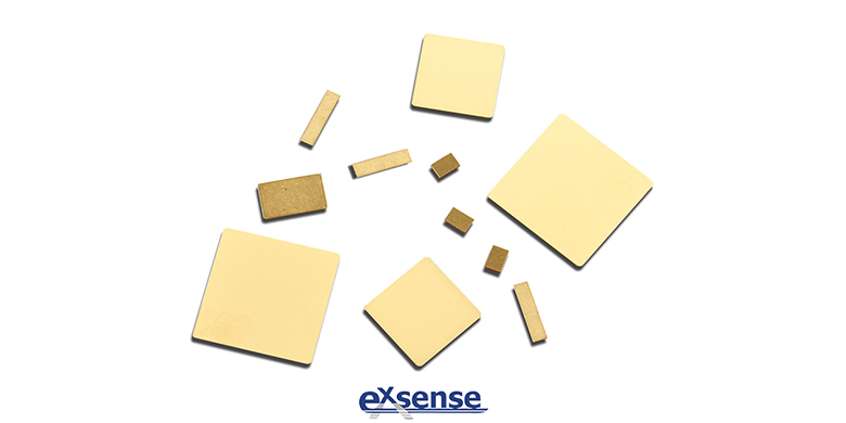
Single layer capacitor researched, developed and produced by EXSENSE Electronics Technology Co., Ltd. has good shape coefficient and is suitable for printed circuit board, chip carrier with limited space, integrated circuit in encapsulating components, etc. Its size can match the chip carrier containing integrated circuit or the limitation in printed circuit board.
In the conventional process, the single layer capacitor is usually fabricated by metallized sintered ceramic material and diced according to the parameter requirements. Although the shape coefficient of single layer capacitors produced according to existing technology is up to standard, the available capacitance limits its application scope, especially when the application scenario requires extremely small or thin single layer capacitors. In this case, the chip capacitor must have high structural strength and high capacitance value. EXSENSE Electronics introduces a single layer capacitor with high capacitance value, high structural strength and high cost performance, which includes ceramic dielectric material and metal electrode layer on the upper and lower surface. The single layer capacitor has at least one internal electrode extending through a part of the width of the ceramic dielectric material and electrically contacting the conductive metallized layer; The conductive metallized layer is located on one side and at least one part of the upper or lower surfaces of the ceramic dielectric material, and another electrically isolated metallized pad is located on the upper or lower surface and electrically contacted with the electrode. Among them, there are several metalized pads electrically isolated from each other on the upper or lower surface of single layer capacitor with high capacitance value. Metallized pads are available in different sizes.
The preparation method of single layer capacitor with high capacitance value is as follows:
One or more electrodes are placed between layers of a ceramic dielectric substrate in the body state;
Cut or drill holes and fill along the edge of the ceramic dielectric substrate of the body;
The upper metal electrode layer and the lower metal electrode layer are printed on the ceramic dielectric substrate in the body state;
The ceramic dielectric substrate in the body state is diced into single layer capacitors with independent high capacitance value;
Sintered single layer capacitance with high capacitance values.


