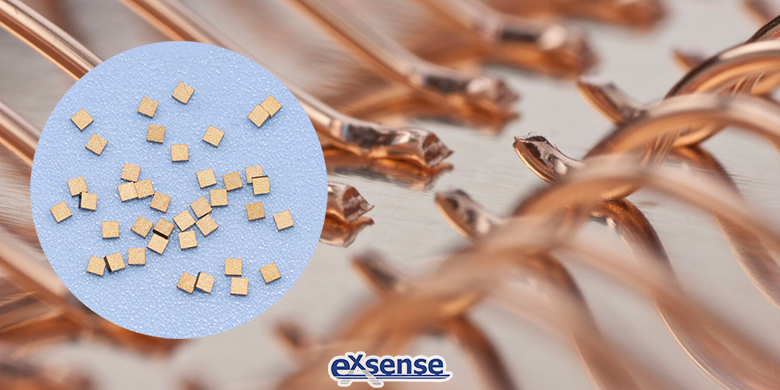
High-accuracy NTC thermistor chip (can up to ±0.5%, ±1%, ±2%, ±3%) produced by EXSENSE Electronics Technology Co., Ltd. is usually used in IGBT module, optical communication module, infrared thermistor printing first class in the form of bonding due to the characteristic that the resistance value changes with temperature.
In the chip bunting technology, copper wire bunting instead of aluminum wire bonding has become one of the important milestones in the history of semiconductor industry, and has made great achievements in the development of semiconductor technology. However, in the field of power semiconductor, copper wire bonding has not been widely introduced and applied. Its market share is less than 1% and it still faces many process problems.
A necessary condition for the use of copper wire bonding is that the surface metallization of NTC thermistor chip also needs to be adjusted. For power semiconductor, aluminum is generally used for surface metallization of thermistor chip, while aluminum is soft and copper is hard, so direct bonding cannot be realized. Could it be changed to a stronger metal layer? Experiments have found that copper is a very suitable metal, and it is very suitable for copper wire or copper tape to be connected on its surface. In addition, power semiconductors generally use larger diameter wire, which requires a certain thickness of surface copper metallization, that is, the so-called thick copper process. However, the metallization process of (thick) copper surface currently has the following problems:
First, electroplating process(ECD) is commonly used in surface copper metallization. Copper, as a diffusion metal, has high solubility and diffusion coefficient, which can diffuse rapidly at lower temperatures and can diffuse to the silicon dioxide layer, then into the silicon and introduce deep trap levels into it. This results in the decrease of life of minority carrier and the increase of node leakage current, the decrease of device performance, reliability and even failure;
Second, in the production process, copper is easy to oxidize under air and low temperature environment (< 200℃), and it cannot form a dense protective layer to prevent further oxidation and corrosion like zinc and nickel;
Third, copper has poor adhesion to silicon oxide and is easy to peel off. However, the wiring required for power semiconductors is relatively thick, which requires a certain thickness of surface metallization to ensure that the bonding process can withstand greater pressure and power, while the thick copper process will lead to more serious stripping problems.
Fourth, the production equipment is expensive, it is difficult to accumulate a certain thickness of copper atomic layer, the cost is very high.
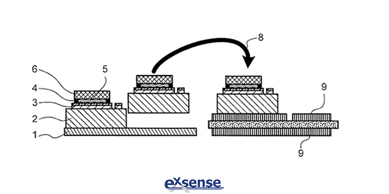
For copper wire bonding process, the difficulties and problems are not in the bonding itself, but in the surface of thermistor chip needs to use copper to achieve the bonding process. Danfoss BondBuffer (DBB), the literal meaning is the bond buffer layer, and the copper wire is bonded on this Buffer layer, which means that there is no copper metallization process on the surface of thermistor chip, so as to avoid the above problems. For this technology, Danfoss basically includes the typical processing technology of this process: directly attaching Buffer copper layer and sintered material to the wafer; The chip with the Buffer copper layer but not sintered is placed on the DBC; Then, the whole process of sintering once from top to bottom, as shown in the following figure:
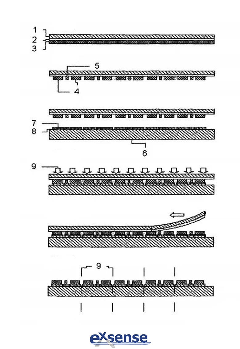
First, a whole Buffer copper layer (3) is fixed on a bracket (1); According to the distribution and shape of the chip on the wafer, the Buffer copper layer is made into the shape corresponding to the chip. The surface of the chip (6) is precoated and sintered silver composite layer (7); The Buffer layer is then pressed against the wafer and removed from the support. After processing on the wafer is completed, the chip needs to be removed from the wafer and placed on the DBC, as shown in the following figure to complete the integration of chip (2) on the DBC, then the overall sintering process is carried out. At the same time, the chip surface has a fairly thick copper metallization layer, then copper wire bonding process.
For power semiconductor modules, the greatest significance of the introduction of copper wire bonding is to improve reliability and actual operating temperature. In addition, there are a number of reliability and performance improvements:
First, the power cycle capacity enhanced;
Second, the internal impedance reduced;
Third, the thermal resistance reduced;
Fourth, improve the aging of welding layer and hollow problems;
Fifth, improve the surface current distribution of thermistor chip;
Sixth. improve the surface temperature distribution of thermistor chip.
Among them, the impedance reduction is due to the lower resistivity of the copper material; The reduction of thermal resistance is due to the sintering process used in the back connection of the NTC thermistor chip; In the same way, due to the introduction of sintering processes for aging of the welding layer and the hollow problems.