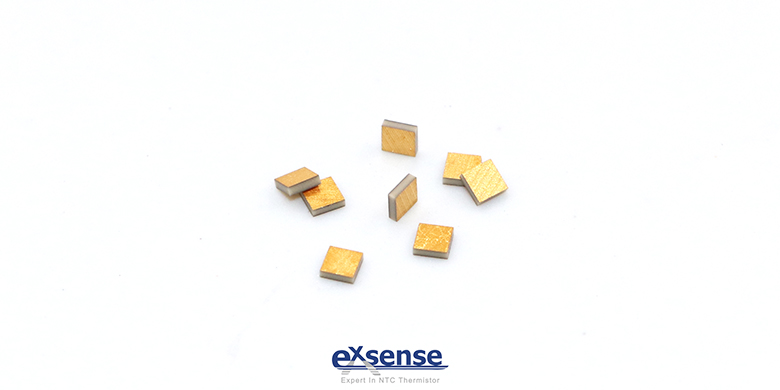
The single layer capacitor produced by EXSENSE Electronics Technology Co., Ltd. has the advantages of small size, thin thickness(0.15~0.5mm), low equivalent series resistance and low loss. Its application frequency can up to GHz, which is suitable for small or microwave occasion and microwave integrated circuit with functions of blocking direct current, RF by-pass, smoothing, tuning, etc.
Ceramics are one of the most useful classes of dielectric materials for chip capacitor. However, due to their fragility and the difficulty in firing them at thicknesses much below 0.004 inch, ceramics are usually used in multi-layer form. This causes high inductance; And this also cause an undesirable property, relative to single layer devices, this is not desirable. Once a given dielectric is selected the size of the resulting device for any given capacitance is conventionally determined by the number of layers and their thicknesses. True single layer capacitor has lower inductance and thus higher resonant frequencies than their multi-layer counterparts and, as stated, are useful at higher frequencies, a necessity for many of today's broadband, wireless and other applications. Since single layer capacitor has a much more limited capacitance range than multi-layer devices, when area is predetermined; e.g., by a circuit configuration, it is very important to get the dielectric thickness as low as possible. True single layer capacitor currently available is limited to about 0.004 inches in minimum thickness because of the fragility of the dielectric materials at lesser thickness. Today, let’s introduces a method of manufacturing single layer capacitor - Ceramic-Metal Composite Method, wihch can avoid high inductance and make thin chip capacitors more widely used when the thickness of capacitor is smaller than 0.001 inches.
Green ceramic tape serves as a precursor for the dielectric layer of the finished chip capacitor, which will be cast to proper thickness for providing the desired fired thickness. The metal and ceramic powders are suspended in a plastic vehicle with solvent to attain the desired viscosity. A small amount of flux may be added to improve wetting characteristics and/or promote adhesion of the paste to the dielectric tape. The paste is applied to the thin green ceramic tape by stencil, screen-printing or other suitable method at a thickness that will assure the physical integrity of the finished product. This paste is prepared by standard processes such as passing the ingredients several times through a three-roll mill.
The green tape and paste, as work-in-progress, are then subjected to thermal processing (firing) that results in a thin dielectric layer adhering to a conductive electrode (or two electrodes). The green tape typically shrinks 10% to 30% in a high temperature furnace depending on its composition. Depending on the dielectric's composition and subsequent firing conditions, the metal in the paste may be either noble or non-noble. For air firing the metal may be platinum, palladium, gold, silver, alloys of these, or others that do not react with the air. Metals such as nickel and copper may be used for non-oxygen firing. Oxidation of the metal must be avoided. The ceramic powder in the paste is, for example, a single compound or a combination of compounds. The ceramic powder can comprise metal oxides and/or titanates, similar to those used for the dielectric in other manufacturing methods. The ratio of metal to powder in the paste can range from about 0.4 grams to 9 grams of metal per gram of powder.
The paste is precursor to finished chip capacitor and is initially applied to one or both sides of the dielectric green tape as required by the design of the particular device being manufactured. When the paste is applied only on one side, a thin solid or patterned layer of co-fireable metal may be applied to the other side of the tape that, when fired, becomes the counter electrode. Alternatively, the counter electrode may be applied after firing by any standard method; e.g., plating, sputtering, screen-printing, etc. The metal powder in the paste is chosen so that it does not melt nor react with the dielectric at its sintering temperature, but forms a strong electrically conductive bond with it. The ceramic powder in the paste is selected so that it imparts physical strength to the sintered product while at the same time does not significantly diminish the electrical conductivity of the metal in the ceramic to metal ratio that is employed.
The entire paste composition is such that shrinkage of the layers' planar surfaces during the burnout/sintering process matches the shrinkage of the dielectric green tape. After application of the paste to the dielectric tape, the tape and electrode(s) paste are co-fired at the prescribed temperature for the given ceramic composition. After the firing process with paste on only one side of the tape, the counter electrode is applied and any required desired pattern etching is done. The composite electrode may also have a thin conductive layer applied to its outer surface by methods such as plating, sputtering, etc. The total after-firing thickness of the dielectric plus two electrode layers should be about 0.003 inch or more (0.004 is preferred) to allow advantageous handling characteristics. After firing, the individual devices are separated by dicing and subjected to normal and customary processing. The devices thus formed will have, after shrinkage in firing, a thin (0.0004 to 0.0015 inch) stratum of dielectric material sandwiched between adherent conductive electrodes either extending to the extent of the chip surface or to a lesser extent leaving a margin of unelectroded dielectric.
Thus, chip capacitor is formed with capacitance values up to about 10 times (or more) the value of a conventional single layer capacitor of their size, by virtue of the actual dielectric after firing being a fraction as thick as the conventional device. Capacitance is further enhanced by the fact, observable with an electron microscope, that the electrode(s) penetrate into the body of the dielectric, further reducing the effective dielectric thickness.At the same time, temperature stability, losses, of this manufacturing method are better than those of conventional single layer capacitor.
Reference Data:
SINGLE LAYER ELECTRONIC CAPACTORS WITH VERY THIN DIELECTRICS AND METHODS TO PRODUCE SAME
US 6, 690, 572 B2
Inventor: Larry A. Liebowitz, 129 Adirondack
Ave., Spotswood, NJ (US) 08884
Notice: Subject to any disclaimer, the term of patent is extended or adjusted under 35 U.S.C. 154(b) by 0 days.
Appl. No.: 10/090,816
Filed: Mar. 6, 2002
Prior Publication Data
US 2003/0169555 A1 Sep. 11, 2003
Int. Cl.7 ............................. H01G 4/06; H01G 4/00
U.S. Cl. ............................. 361/311; 361/303
Field of search ............................. 361 /301.4, 303-305, 361/311-313, 320,321.1-321.5
References Cited
U.S. PATENT DOCUMENTS
3, 689, 810 A * 9/1972 Walles ........................ 361/305
3, 882, 059 A * 5/1975 Elderbaum ................. 29/25.42
5, 254, 360 A *10/1993 Crownover et al. .......... 427/79
5, 737, 180 A * 4/1998 Yoo ............................. 361/313
6, 207, 522 B1 * 3/2001 Hunt et al. .................... 438/393
6, 366, 443 B1 4/2002 Devoe et al. ..................... 361/313
6, 433, 993 B1 * 8/2002 Hunt et al. ..................... 361/303
FOREIGN PATENT DOCUMENTS
P-2000-327964 A * 11/2000
cited by examiner
Primary Examiner - Dean A. Reichard
Assistant Examiner - Eric Thomas
Attorney, Agent, or Firm - Leonard Cooper