Single layer capacitor is widely used in electronic countermeasures (ECM), radar, satellite communication (SATCOM), etc., and which has the characteristics of large capacitance and wide appliance. With the continuous progress of science and technology, higher requirements are put forward for the quality and reliability of single layer capacitor. At present, the single layer capacitor prepared by ordinary method is characterized by defects such as high loss of efficiency, low pass rate and low reliability. Especially during the preparation process, the defects such as the porosity defect in ceramic preparation, the low adhesion in ceramic metallization and the mechanical damage in the matrix caused by the cutting process seriously affect the reliability of the products and which are difficult to meet the needs of customers.
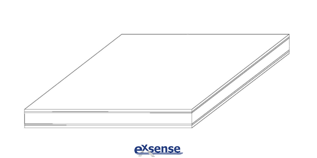
In order to solve the above technical defects, EXSENSE Electronics introduces a single layer capacitor and its preparation method, which includes the first electrode plate, the second electrode plate and the substrate ceramic layer. The first electrode plate consists of the first gold electrode layer, the first nickel electrode layer and the first titanium-tungsten-alloy transition layer laid in turn; The second electrode plate is composed of the second gold electrode layer, the second nickel electrode layer and the second titanium-tungsten-alloy transition layer laid in turn. The specific preparation methods are as follows:
First, the appearance inspection and water absorption rate detection of substrate
Check whether the surface color of dielectric ceramic substrate is uniform, smooth, no cracks, burrs, etc.; At the same time, the water absorption rate of the dielectric ceramic substrate should be within the range of 0.08%~0.35%.
Second, cleaning ceramic substrates
Rinse the wash box used for substrates cleaning with ionized water; The ceramic substrates are put into the wash box and cleaned with anhydrous alcohol. The ultrasonic voltage is adjusted to 150±50V and the cleaning time is 20±2mins. After that, the ceramic substrates are gently cleaned with a cotton swab; Then put them into the ultrasonic cleaning machine for cleaning with cleaning agent (concentration is 5%). The ultrasonic output voltage is adjusted to 150±50V, and the cleaning time is 20±2mins, all substrates must be immersed; Finally, they are cleaned with ionized water for 20±2mins and then washed in a water bath furnace which is heated to 100±3℃. After cleaning, remove the substrates.
Third, sintering
All substrates are sintered in a high-temperature furnace, the sintering temperature is 600±100℃, and the holding time is 60±30mins.
Fourth, vacuum sputtering
Sputtering parameters are set to heat the sputtering machine chamber at a temperature of 150℃~400℃. The substrate adopts rotation and revolution mode to improve the film thickness. DC sputtering is adopted for sputtering. Meanwhile, an online monitoring system is adopted to monitor the sputtering film thickness in real time. First sputter the transition layer titanium-tungsten-alloy target material, then sputter Au target material, and then sputter Ni target material. Among them, the vacuum degree of titanium-tungsten-alloy target material in the sputtering transition layer is 9.0*10-3~1.0*10-5Pa, the sputtering power is 200W~600W, and the sputtering time is 100s~600s. The vacuum degree of sputtering Au target material is 9.0*10-3~1.0*10-5Pa, sputtering power is 200W~600W, sputtering time is 800s~1200s. The vacuum degree of sputtering Ni target material is 9.0*10-3~1.0*10-5Pa, sputtering power is 200W~600W, sputtering time is 2800s~3800s. After the vacuum sputtering is completed, turn off the heating device and remove the substrates after the furnace cools for at least 8h.
Fifth, heat treatment
Vacuum heat treatment is carried out on the substrate completed by sputtering, the vacuum degree is higher than 10-2Pa, the vacuum heat treatment temperature is 200℃~700℃, and the heat treatment time is 20~72h.
Sixth, cutting
Ceramic substrates are bonded to the blue plastic film,set the spindle speed and cutting speed for cutting. Among them, the spindle speed is set as 26,000~34,000 RPM/min, the cutting speed is set as 0.3~0.8mm/s. When cutting, firstly cut the sample, then adjust the cutting size parameters according to the electrical properties of the sample product to improve the hit ratio of the product. After cutting, remove the leftover material; Dehydrated with alcohol at temperature of 70℃~150℃, and the drying time is set as 30mins.
Seventh, sort
The single layer capacitor is sorted for appearance, electrical capacity and loss, the defective products are eliminated.
Eighth, the chip capacitor is screened by 100% temperature shock and voltage treatment.
Ninth, packaging
Pack the product into a waffle tray and pack it in a box.
This single layer capacitor and its preparation method adds the test of substrate water absorption rate on the basis of the traditional manufacturing method, add the substrate sintering process after the substrate cleaning process to further remove impurities, effectively screen the substrate quality and improve the electrode adhesion in the vacuum sputtering process. At the same time, online test system was added in the key process of vacuum sputtering, which effectively controlled the sputtering layer thickness of various materials, avoided the influence of equipment parameter fluctuation, and improved the consistency and reliability of products. In the process of ceramic metallization, full sputtering is adopted to reduce the influence of electroplating process.