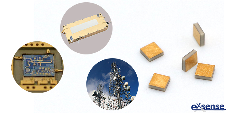
Chip capacitor, because of its small size, large electrical capacity, good consistency, is widely used in microwave communication lines, microwave power amplifiers and microwave integrated circuits, plays the roles of straight-through, RF bypass, filtering, tuning, etc.. The preparation process of the existing chip capacitor is mostly for ceramic powder mix →ball milling→ isostatic pressing molding →ceramic ingots sintering→ slices→ silver electrode printed by silk-screen printing method→ drying→sintering→ dicing. However, there are the following problems with the chip capacitor made by this process:
First, in the environment of hot and cold impact, when the metal electrode of chip capacitor is welded with solder at high temperature, the temperature near the welding spot will suddenly change, and the stress caused by thermal expansion and cold contraction of the metal electrode will easily make it crack, which will affect the appearance of the product;
Second, due to the thermal expansion coefficient of the metal electrode and ceramic substrate is different, their different of expansionary and contracted degree is also result in stress, this stress can not be released on the firm welding spot, which is easy to cause micro-crack or even fracture of ceramic substrate, which greatly affects the performance of chip capacitance, reduce its reliability and stability, resulting in a lower qualified rate of products, increased production costs.
In order to solve the above problems, EXSENSE Electronics recommends a stress buffer metal electrode chip capacitor, which has the advantages of heat and cold shock resistance, structural stability and high reliability. The chip capacitor consists of a ceramic substrate and two composite electrodes located on two surfaces of the ceramic substrate, which are made of a first metal electrode layer, a stress buffer layer and a second metal electrode layer stacked from the inside out on the ceramic substrate surface, and the stress buffer layer made of material mixed with metal slurry and kaolin powder.
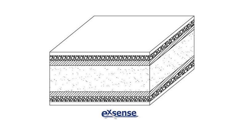
Compared to the existing chip capacitor, this chip capacitor uses a composite electrode structure of the first metal electrode layer - the stress buffer layer - the second metal electrode layer. Among them:
The first metal electrode layer is combined with the ceramic substrate, which is not easy to fall off the surface of the ceramic substrate, and its thickness is 3 to 20 μm.
The stress buffer layer is prepared with a metal slurry with kaolin added, which has a loose multihole structure similar to a sponge, which can cushion the stress caused by changes in the external environment and protect the first metal electrode layer and substrate from stress damage. It can improve the stability and reliability of chip capacitor as a whole, and the stress buffer layer also has a certain barrier effect. In the material of the stress buffer layer, the mass ratio of kaolin powder to metal slurry is 1 to 20:100. The performance of the stress buffer layer made under this scale range is more suitable, if the amount of kaolin is too small, it is difficult to form a spongy loose multihole structure, the stress buffer layer does not play the role of buffer stress; If the addition is too much will affect the adhesion of the stress buffer layer, thereby affecting the reliability of the chip capacitor. Depending on different metal slurry, the amount of kaolin added is adjusted accordingly in this proportion range. The thickness of the stress buffer layer is 3 to 20 μm. The performance of the stress buffer layer in this thickness range is more suitable, too thin can not act as a buffer, too thick increases the cost, but also may affect the reliability of the chip.
The second metal electrode layer, as a surface welding layer, has a welding effect, and its thickness is 0.1 to 1 μm.
The preparation methods for the stress buffer metal electrode chip capacitor are as follows:
S1: Preparation of ceramic substrates:
The ceramic powder is prepared according to the conventional chip capacitor formula, and then the ceramic powder is ball-milling, isostatic pressing molding, sintering and slicing to obtain the flaky ceramic substrate.
S2: Printing the first metal electrode layer:
The metal slurry is printed on two surfaces of ceramic substrate by silk-screen printing method. After the metal slurry is dried, the first metal electrode layer is printed on the ceramic substrate.
S3: Print stress buffer layer:
Kaolin powder is added into the metal slurry in accordance with the ratio, fully stirred evenly then print on the surface of the first metal electrode layer by silk-screen printing method, then dried and sintered at 700~1000℃ to obtain the stress buffer layer printed on the surface of the first metal electrode layer.
S4: First cleaning:
The ceramic substrate is treated with cleaning liquid, and then cleaned by ultrasonic machine. The cleaning time is 5±1 minutes, and then dried. The drying temperature is 100±5℃, and the drying time is 30±5 minutes.
The ceramic substrate is treated with cleaning fluid and then washed with an ultrasonic machine for 5±1 minutes, then drying at a drying temperature of 100±5 degrees C and drying time of 30±5 minutes.
S5: Second cleaning:
The ceramic substrate obtained from the first cleaning is put into the plasma cleaning machine for the second cleaning, the cleaning time is 5±1 minutes, the drying temperature is 100±5℃, the drying time is 30±5 minutes, and the surface is activated at the same time.
S6: Sputtering the second metal electrode layer:
The vacuum sputtering coating machine is first vacuumed into the process range, then filled with argon as the working gas, and precious metal as the target material. Under the action of electric field, Ar+ accelerated the bombardment of the target material, and the target atoms are sputtered onto the ceramic substrate, and the first and second metal electrode layers are sputtered on the stress buffer layer of the two surfaces of the ceramic substrate.
S7: Dicing:
The ceramic substrate is diced to obtain a single chip capacitor.
Stress buffer metal electrode chip capacitor resistance to cold and hot shock, in cold and hot shock environment, such as high temperature welding, when stress buffer layer can greatly reduce the destructive stress to the ceramic substrate and the first metal electrode layer, stress of the composite electrode on the whole is less effective, which is not easy to crack, and the ceramic substrate is also less likely to crack under stress, so as the structural stability and reliability of the capacitor are improved, It can guarantee the reliability of chip capacitor and minimize the cost.