In the development of modern electronic field, the miniaturization and multi-function of electronic devices have become the development trend, and the increasing demand for chip electronic components in the electronic field drives the rapid development of SLC single layer capacitors. Grain boundary layer semiconductor ceramics have the advantages of great temperature characteristic, high dielectric constant and great frequency characteristic, etc., and play an important role in single-layer chip semiconductor ceramics. The production process of the existing grain boundary layer semiconductor ceramic materials is generally as follows:
Material ratio → mixing with deionized water → drying → crushing → calcining → sieving → adding additives → mixing → flow forming film → discharging glue → reduction in hydrogen and nitrogen mixture → oxidizing agent coated, oxidation in air atmosphere, sintering → substrate for single layer capacitor.
Most of the grain boundary layers prepared by this process are added with heavy metals such as cadmium and lead, which will pollute the environment greatly in the process of production and use. In view of the defects of the existing technology, EXSENSE Electronics Technology Co., Ltd. introduces a high dielectric constant SLC single layer capacitor. The semiconductor ceramic material of the grain boundary layer does not contain heavy metals such as cadmium and lead, which has the advantages of less environmental pollution and high dielectric constant. The high dielectric constant SLC single layer capacitor is composed of 60~ 69% SrCO3, 30~ 38% TiO2 and 0.2~ 3% additives by weight percentage. The specific preparation method is as follows:
First, mix the SrCO3 and TiO2 according to the ratio, add the deionized water, then ball grinding machine is used for mixed ball grinding; The weight ratio of powder, grinding ball and deionized water in the ball grinding slurry is 1:5:1~1.5, and the ball grinding time is 2~3 hours, then dried, crushed;
Second, the powder is calcined in 1200℃~1300℃ for 3~4 hours, then crushed, sieved;
Third, add additives in the powder, add deionized water, then ball grinding machine is used for mixed ball grinding; The weight ratio of powder, grinding ball and deionized water in the ball grinding slurry is 1:5:1~1.5, and the ball grinding time is 3~4 hours, then dried, crushed, 60 mesh sieved;
Fourth, the powder is pressed into 50mm*50mm ingots under the pressure of 20~30MPa, then sintered to get the ceramic body, the sintering conditions are: temperature insulation sintering for 4~5 hours first in the hydrogen and nitrogen mixed atmosphere at 1300℃~1400℃, then cooled to 1000±50℃ and air insulation sintering for 3~6 hours;
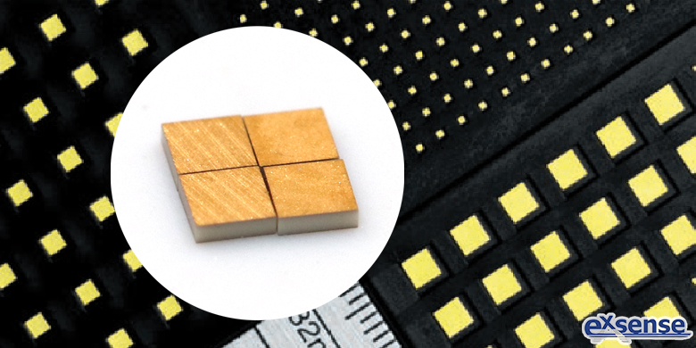
Fifth, the ceramic substrate for single layer capacitor is obtained by slicing the ceramic body according to the required thickness;
Sixth, the ceramic substrate is metallized by printing or sputtering, metal electrode is formed on the ceramic substrate;
Seventh, the ceramic substrate is diced by a dicing machine to obtain the single layer capacitors;
Eight, test the electrical performance of single layer capacitor.
High dielectric constant single layer capacitor through reasonable ratio such as ZnO, CaCO3, Li2CO3, B2O3, CuO, La2O3, SiO2, Bi2O3, additives, etc., forming a stable and well-insulated grain boundary layer on the grain boundary, so the same insulating performance can be achieved without coating insulating oxide. In addition, by adjusting the sintering process, the semiconductor ceramic material of grain boundary layer of ceramic capacitor with good performance can be produced by one sintering, the secondary sintering process coated with insulating oxide is not required, reduce the cost of production, and is in line with the development trend of miniaturization and high capacity of single layer capacitor to meet the increasing technical needs.