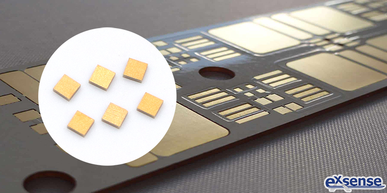
SLC single layer capacitor has the characteristics of small size, large capacity and high application frequency, etc., which are widely used in electronics, radar, navigation and satellite communications, etc.. In the traditional single layer capacitor, there is a dielectric layer in the middle, and an upper and lower layer of electrode layer. The lower electrode is welded on the circuit with the solder such as gold-tin alloy or lead-tin alloy, and the upper electrode is connected to other circuit components with the gold wire bonding technology.
At present, the preparation process of gold-tin solder of single layer capacitor is either low material utilization rate, which greatly increases the production cost; Or the process difficulty coefficient is high, the control requirements of composition and temperature of electroplating tank liquid are very high, and there are problems such as electroplating solution pollution, it is difficult to meet the environmental requirements. In order to solve these problems, EXSENSE Electronics Technology Co., Ltd. introduces a single layer capacitor with gold-tin solder, which includes gold-tin solder layer, lower electrode layer, medium dielectric layer and upper electrode layer. The chip capacitor can improve the encapsulating efficiency and reduce the encapsulating cost; Which is simple process, controllable speed, low production cost; The whole process is pollution-free, and the welding performance of the made of gold-tin solder in high temperature is excellent, to ensure the stability of the product, which is suitable for industrial production.
The specific preparation steps of single layer capacitor with gold-tin solder are as follows:
First, prepare ceramic substrates, clean and dry;
Second, the electrode layers formed on the upper and lower surfaces of ceramic substrate with evaporation method or sputtering method;
Third, the ceramic substrate forming the upper and lower electrodes is put into the vacuum sputtering machine, the gold-tin solder layer is sputtered by DC sputtering, the substrate is sputtered by rotation and rotation;
Fourth, sputtering gold-tin solder layer, the target material is made of gold-tin alloy with mass ratio 80: 20, cavity heating temperature is 100~500℃, vacuum degree is 10-6-10-7mTorr, power is 500W~4000W, time is 50 ~1000s, using X-ray machine or step profiler monitoring sputtering film thickness, at the same time using online monitoring system to monitor real-time sputtering film thickness;
Fifth, according to different ceramic substrate performance requirements, part of the substrate only needs to sputter gold-tin solder layer on the surface of the upper electrode or the lower electrode, and part of the substrate needs to sputter on both sides;
Sixth, after sputtering, turn off the heating device, fill in the gas, and take out the semi-finished product;
Seventh, the semi-finished products are processed by conventional lithography, etching, electroplating, cleaning and other processes;
Eight, dicing, test, sorting;
Ninth, product packaging.